The First Trillion Transistor Chip a New Design Space
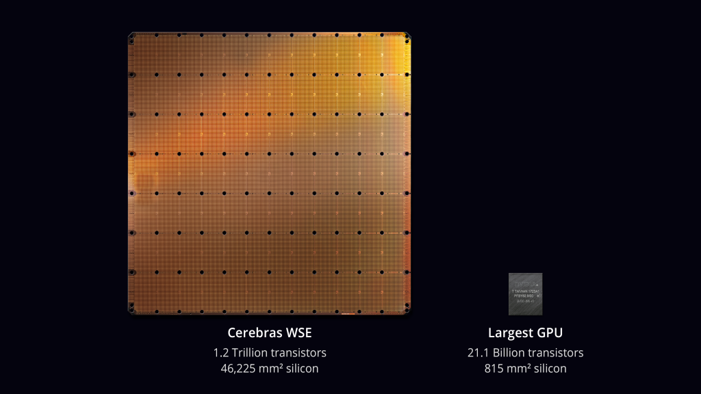
There was stunning news at the HotChips-31 conference held at Stanford Memorial Auditorium last week. Cerebras, a startup company working on machine learning accelerators in stealth mode, finally came out and presented a groundbreaking accelerator chip packed with 1.2 trillion transistors on a single die (46,225 mm2), the first time in human history. Based on TSMC 16 nm process node, this mousepad-sized single die named WSE — stands for Wafer Scale Engine and pronounced "wise" — houses 400,000 processing cores optimized for AI/ML processing with a whopping 18 GB on-die scratchpad SRAM at 15 to 50 kW. The first moment we heard about the wattage, the reaction was "you must be kidding me!"
The immediate challenges from a designer's perspective are: how do you deal with packaging, manufacturing yield (no chip is perfect), the power delivery to the chip, the power density, and the heat dissipated from the giant chip. Cerebras received $111 million in VC funding, enough to design their own heat dissipation apparatus and unconventional test equipment and probe stations. To achieve this bold, remarkable feat, which I'd like to call a " supercomputer-on-a-wafer ," Cerebras designers must have worked out the feasible fabrication and packaging technologies with their manufacturer TSMC years before investing in their significant design effort. More recently, an HPCA 2019 paper proposed a similar solution. With this technology, functional integration will become more natural and efficient from a communication standpoint, as we'll discuss next.

Cerebras WSE Chip vs. NVIDIA GPU (Source: Cerebras)


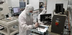
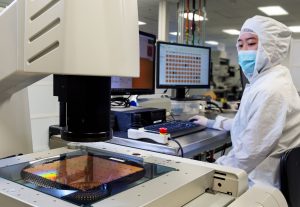
Cerebras in-house test equipment and probe station (Source: Cerebras)
Disappointingly, but not surprisingly, other than saying WSE is optimized for sparse linear algebra with specialized tensor units and "sparsity harvesting", Cerebras did not disclose any further information on the aggregated performance potential of the chip nor the power efficiency (e.g., TOPS/Watt). They simply said "it's working and running several customers' workloads" during their HotChips presentation. I believe these performance numbers will be used later to set their pricing strategy for this unprecedented chip. By sparsity harvesting, it sounds like Cerebras WSE is capable of eliminating ineffectual computation with dynamic zero compression in the vectors and matrices.
Process Variation
While fabrication defect issues can be addressed by redundancy and wiring bypass post-manufacturing, as mentioned by Cerebras' co-founder Sean Lie, process variation is another tricky issue not discussed in his talk. This can be especially problematic when the transistor feature size continues to scale down to 7 nm (today), 5 nm (very near future), and below. In layman's terms, transistors at this scale are not created equal due to dopant diffusion fluctuation, varied oxide thickness, lithographic artifact, etc. In general, in order to guarantee targeted performance and yield, chip designers must consider intra-die variation, usually with a maximum die size of a typical reticle (~815 mm2). With Cerebras' die size of 46,225 mm2, all the inter-die variation now turns into an intra-die variation problem. The operating frequency will likely be penalized by the slowest transistor region even though the faster regions can be cranked up to run at a higher frequency if they are cut at a finer-grained size off the wafer. To address this shortcoming, they might employ GALS design on their NoC-interconnected cores to allow different core groups to run asynchronously.
Power Delivery
Further, such an enormous chip will face tremendous challenges in the physical design space. Among the top issues are clock distribution/clock skew and IR drop. Minimizing clock timing skew to ensure synchronous operations of all digital blocks is already an arduous feat for modern circuit designers. A large chip with long wire paths only makes the problem much more challenging. Long wires also exacerbate the overall resistance, aggravating IR drop. Ill-managed IR drop can slow the circuit operations down as the supply power to each functional unit is being trickled down over a long resistive wire path. In the worst case, it can lead to circuit malfunction if the voltage drops way below the operational nominal. Cerebras did mention their unique technique to supply and deliver power in the Z-direction, using perpendicular power wires. Assuming that this is feasible, the power grid can probably receive supply voltage more uniformly and amply from the "sky" at the top.
Thermals
Finally, power density is a critical challenge. Note that the heat removal mechanism in modern processors has been stuck at under 100 watts per cm2 for a while. With a wattage up to 50 kW in WSE, it will exceed this limitation (to 108 watts/cm2) and call for major innovation in dissipating heat. Similar to their power delivery system, Cerebras claimed the installation of water cooling in the Z-direction, again, using perpendicular water tubes. With all these third dimensional gears, I am sure that the final package of their chip will look incredibly esoteric, like alien technology.
Communication
So why a giant chip versus current multi-accelerator solutions or recent emerging interposer-based chiplet solutions? What are the potential advantages? The answer is clear — the communication. Aside from smaller and faster transistors in feature size scaling, i.e., scaling the FEOL (FrontEnd-Of-the-Line), miniaturization also scales down BEOL (BackEnd-Of-the Line, i.e., the metal layers) to shorten the wire length, although at a much slower pace. Nonetheless, cross-die communication is inevitable where signals will be driven in-and-out through I/O cells across functional dies on the PCB. It is power-consuming and slow. To address the long latency issue and due also in part to yield and form factor concerns, multi-chip-module (MCM), fan-out wafer-level packaging (FOWLP or TSMC's InFO), or the emerging chiplet packaging technology were employed to close the communication gap to different degrees. Cerebras WSE designers took it to another extreme though; they basically shrunk a PCB-level design and mapped it onto a single, large chip. With that, their design converts most of the off-die communication into an on-die transfer network to enable enormous bandwidth for inter-neural-network-layer communication (100 Pbit/s fabric bandwidth), thereby reducing communication latency and wire power substantially. For neural networks, ML practitioners can potentially place and map all the network layers' computation and flow onto the WSE's fabric without leaving the chip. I believe this is the biggest incentive for a giant chip like Cerebras WSE.
If you are old enough, there was a similar attempt back in early 1980, led by the legendary Gene Amdahl (remember Amdahl's Law in Computer Architecture 101?), the chief architect of IBM System/360 whose instruction set is still alive and running more than half a century later. His startup, Trilogy Systems, envisioned a wafer-scale integration solution. The size of the Trilogy chip was roughly 2.5in x 2.5in (4,032 mm2) and employed power-hungry ECL bipolar transistors in exchange for high performance. In other words, the size of Cerebras WSE is 11.5x larger, and each transistor in TSMC 16 nm is about four orders-of-magnitude smaller (in area) than the ~2.5 micron process back in the early 1980s.

Trilogy Systems, circa. 1985 (Source: Wikipedia)
It's great to see that all the collective technology advancement over the years continues to elevate old ideas to new levels of innovation for modern applications. Cerebras, with their partner TSMC, has led the semiconductor industry to a new era with their record-breaking number of transistors on a single chip; it indeed game-changes the landscape of traditional chip designs. In addition to the massive boost of computing power, the enduring memory wall can also be torn down with such a scale of integration, as can communication cost. This prompts new research questions regarding how to repartition on-die transistor assets for general-purpose processors, on-chip memory, special-purpose accelerators, on-chip routers, etc., and how to explore the design space for different application classes. Meanwhile, EDA tools, in particular for physical design, must be enhanced for this design scale for efficient design closure and sign-off. The road ahead in chip design will be more interesting than ever.
About the Author: Hsien-Hsin Sean Lee leads AI Infrastructure Research at Facebook Boston. He previously held positions at TSMC, Georgia Tech, Agere, and Intel. He received appropriate education at the University of Michigan. He is a Fellow of the IEEE.
Disclaimer: These posts are written by individual contributors to share their thoughts on the Computer Architecture Today blog for the benefit of the community. Any views or opinions represented in this blog are personal, belong solely to the blog author and do not represent those of ACM SIGARCH or its parent organization, ACM.
The First Trillion Transistor Chip a New Design Space
Source: https://www.sigarch.org/the-first-trillion-transistor-chip-a-new-design-space/#:~:text=Cerebras%2C%20a%20startup%20company%20working,first%20time%20in%20human%20history.
0 Response to "The First Trillion Transistor Chip a New Design Space"
Post a Comment